
Ceramic Arm for Wafer Drive | Touch-Down Semiconductor Parts
Touch-Down precision ceramic arms for wafer drive with 0.0001-0.0003mm tolerance. ISO 9001 certified semiconductor equipment components for automated wafer handling systems.
Ceramic Arm for Wafer Drive of Semiconductors
Touch-Down produced Ceramic arm for wafer drive of semiconductor feature good structural strength, high temperature resistance, high pressure resistance, good accuracy, good parallelism, high density and uniform organization. For many years, it has been used by the semiconductor manufacturing plant.
Touch-Down boasts a group of excellent engineers and enjoys a unique high-profile technology in the special-shaped ceramic processing projects. Special-shaped processing technology is the strengths of Touch-Down.
Located near the Science Park of Taiwan Hsinchu, the world-renowned science and technology town, our plant enjoys more than 25 years of professional production and processing experience in alumina, zirconia, silicon nitride, silicon carbide ceramic production and processing. We boast strong technical force, refined equipment and rich processing experience. Now we have several precision CNC equipment, precision machine tools, and a variety of leading processing technology and processing tools as well as sophisticated detection equipment to ensure product quality and precision. We are able to produce precision ceramic parts of a variety of specifications, types according to customer drawings. Our products feature high precision, good performance and are widely used in semiconductor, photovoltaic, precision machinery, military, medical, scientific research and other field.
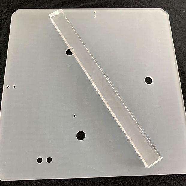
Ceramic Cutting / Grinding Disc (For Semiconductor)
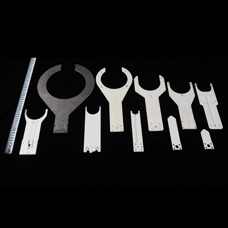
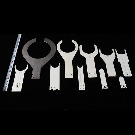
This image shows a set of precision ceramic wafer handling forks used in semiconductor fabrication equipment. These components function as wafer transfer end effectors in automated wafer handling systems, supporting safe movement and positioning of silicon wafers throughout the manufacturing process.
Manufactured from high-purity technical ceramics, these wafer forks provide:
Low particle generation for cleanroom compatibility
High thermal stability for process environments
Excellent mechanical rigidity for precise wafer support
Chemical resistance for semiconductor fabrication conditions
Different fork geometries are designed to support various wafer diameters (150mm / 200mm / 300mm) and equipment architectures, including wafer transfer robots, wafer aligners, wafer inspection systems, and process tool loading modules.
These ceramic components are widely used in semiconductor fabs, wafer handling automation platforms, and front-end wafer processing equipment.
Main Features
Touch-Down produced precision ceramic parts feature good structural strength, high temperature resistance, high pressure resistance, good accuracy, good parallelism, high density and uniform organization.
The Main Products
Ceramic Bolt, Ceramic Shaft, Zirconia Ceramic, Plug Gauge, Ring Gauge, Alumina Ceramic Arm, Ceramic Disc, Ceramic Ring, Microporous Ceramic Vacuum Chuck, Substrate, Ceramic, Ceramic Rails, Special-Shaped Pieces and so on.
- Gallery
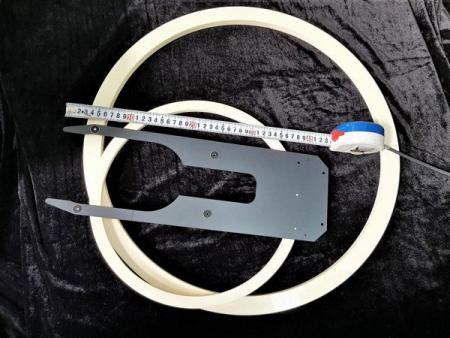 Ceramic wafer ring、Wafer handling ring、Semiconductor wafer transfer arm、Wafer handling robot component、Semiconductor ceramic parts
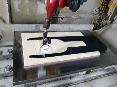 Ceramic arm for wafer drive of semiconductors
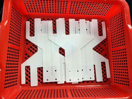 Ceramic arm for wafer drive of semiconductors
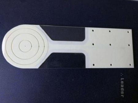 Product Title: Multi-Zone Precision Ceramic Heater for Semiconductor Processing
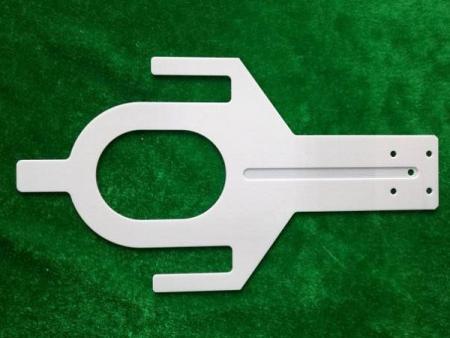 Ceramic arm for wafer drive of semiconductors
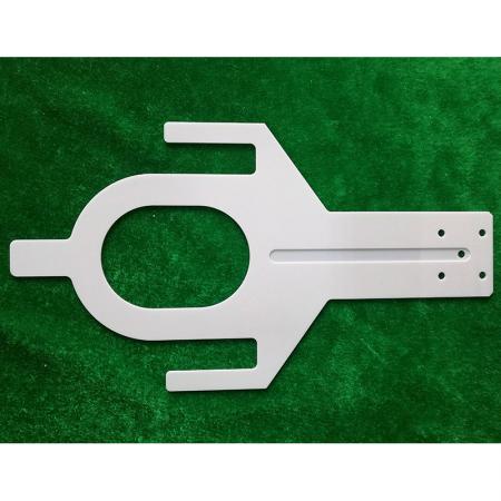
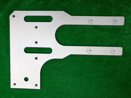 High-Precision Ceramic End Effector (Robot Blade) for Semiconductor Handling. 「Wafer Handling」、「Robot Blade」、「Ceramic Arm」
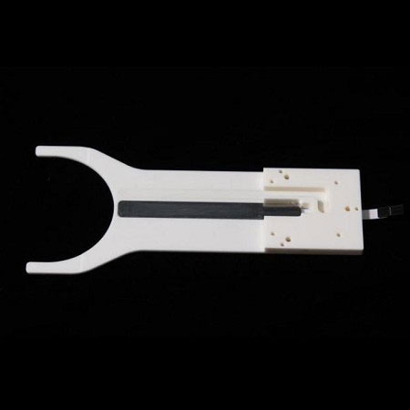
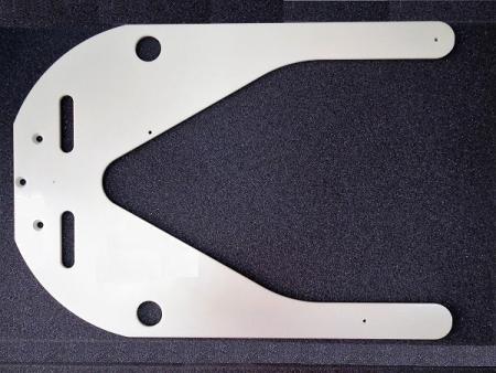 High-Precision U-Shaped Ceramic End Effector (Robot Blade). Ideal for EFEM (Equipment Front End Modules), ALD, CMP, and Dry Etching automation systems.
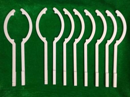 Comprehensive Precision Ceramic Robot Blades & Handling Components. Applications、Equipment Front End Modules (EFEM), Wafer Metrology & Inspection, PVD/CVD processes, Etching, and back-end assembly/test handling.
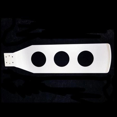
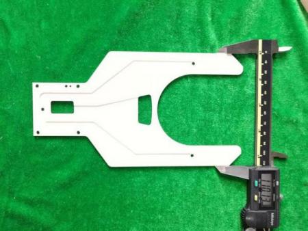 Precision Ceramic Vacuum Blade with Integrated Micro-Channels. Applications,High-throughput automated wafer handling systems, thin-film deposition (CVD/ALD), Lithography tracks, and 300mm wafer processing modules.
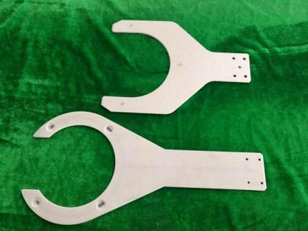 High-Performance Ceramic Robot Blade for Semiconductor Packaging & Testing. Semiconductor packaging equipment, Wafer sorting & testing systems, and high-temperature baking process handling.
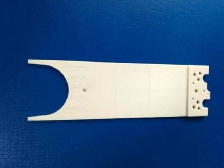 Ceramic arm for wafer drive of semiconductors
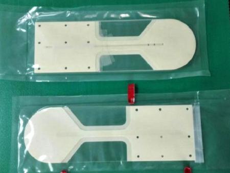 Ceramic arm for wafer drive of semiconductors
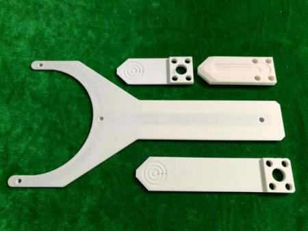 Multi-Series Precision Ceramic Vacuum Chucks & End Effector Assemblies. Applications,Wafer inspection systems, Wafer bonding, Back-end assembly and testing (OSAT), and surface analysis instrumentation.
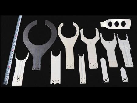 Comprehensive Series of Precision Ceramic End Effectors (Robot Blades). Applications,EFEM automation, CVD, Etching, Diffusion/RTP, and Wafer Metrology/Inspection.
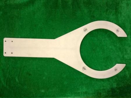 Ceramic arm for wafer drive of semiconductors
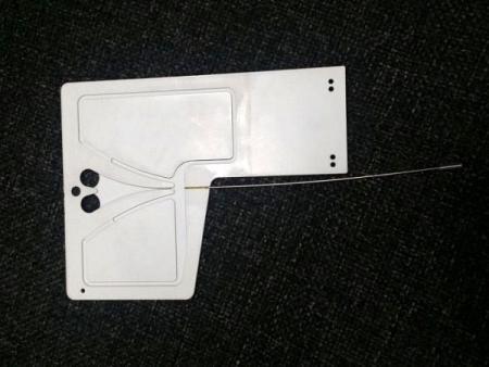 Precision Ceramic Heating & Vacuum Handling Components. Applications: Chemical Vapor Deposition (CVD/ALD), Plasma Etching, Equipment Front End Modules (EFEM), and high-temperature wafer probing.
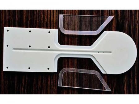 High-Precision Ceramic Robot Blade with Integrated Vacuum Channels. Applications,300mm wafer handling systems, Automated Optical Inspection (AOI), Metrology/Thin-film measurement tools, and High-Vacuum transfer modules.
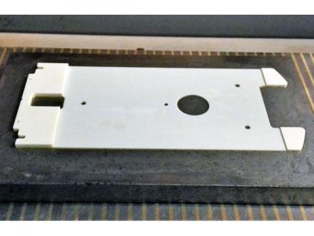 Comprehensive Collection of Semiconductor-Grade Ceramic Robot Blades & Vacuum Chucks. Applications"Equipment Front End Modules (EFEM), High-vacuum chamber transfer, Wafer inspection/metrology, and OSAT automated testing lines."
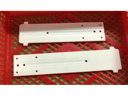 Ceramic arm for wafer drive of semiconductors
- Files Download

Precision Ceramics
Touch-Down - Most accurate and professional long-term partner. Welcome to trial and proofing.
Download
 Download
 Popular Products
How can you ensure zero contamination and maximum wafer handling precision in your semiconductor fabrication process?
Touch-Down's precision ceramic arms for wafer drive deliver ultra-high accuracy with 0.0001-0.0003mm tolerance and low particle generation specifically designed for cleanroom semiconductor environments. Our 29 years of manufacturing expertise and ISO 9001 certification guarantee consistent quality and reliability for your wafer handling automation systems. Contact us today to discuss custom solutions compatible with your existing equipment from Applied Materials, Lam Research, TEL, or Hitachi.
Our special-shaped ceramic processing technology represents a core strength of Touch-Down, enabling custom design and production of ceramic arms tailored to support various wafer diameters (150mm, 200mm, 300mm) and equipment architectures. Whether for wafer transfer robots, wafer aligners, wafer inspection systems, or process tool loading modules, our ISO 9001:2008 certified production facilities combine precision CNC equipment, advanced machine tools, and sophisticated detection systems to ensure consistent quality and reliable lead times. We welcome inquiries with technical drawings or samples and offer comprehensive OEM services and custom solutions that meet the demanding requirements of modern semiconductor fabrication environments.